RTL ASIC SoC Architect / Lead RTL Design Engineer
Location: India (Hybrid/Onsite)
Job Description:
• System & Micro-Architecture Definition: Proven ability to translate product requirements and specifications into scalable, power- and performance-optimized micro-architectures.
• SoC Integration & Sub-System Ownership: Extensive experience in top-level SoC integration, clock/reset architecture, power domain planning, and cross-IP coordination.
• Bus Protocols & Interconnects: Strong expertise in industry-standard protocols such as AXI/AHB/APB, coherent interconnects (ACE/CHI preferred), and peripherals including PCIe, USB, Ethernet, CXL, and DDR.
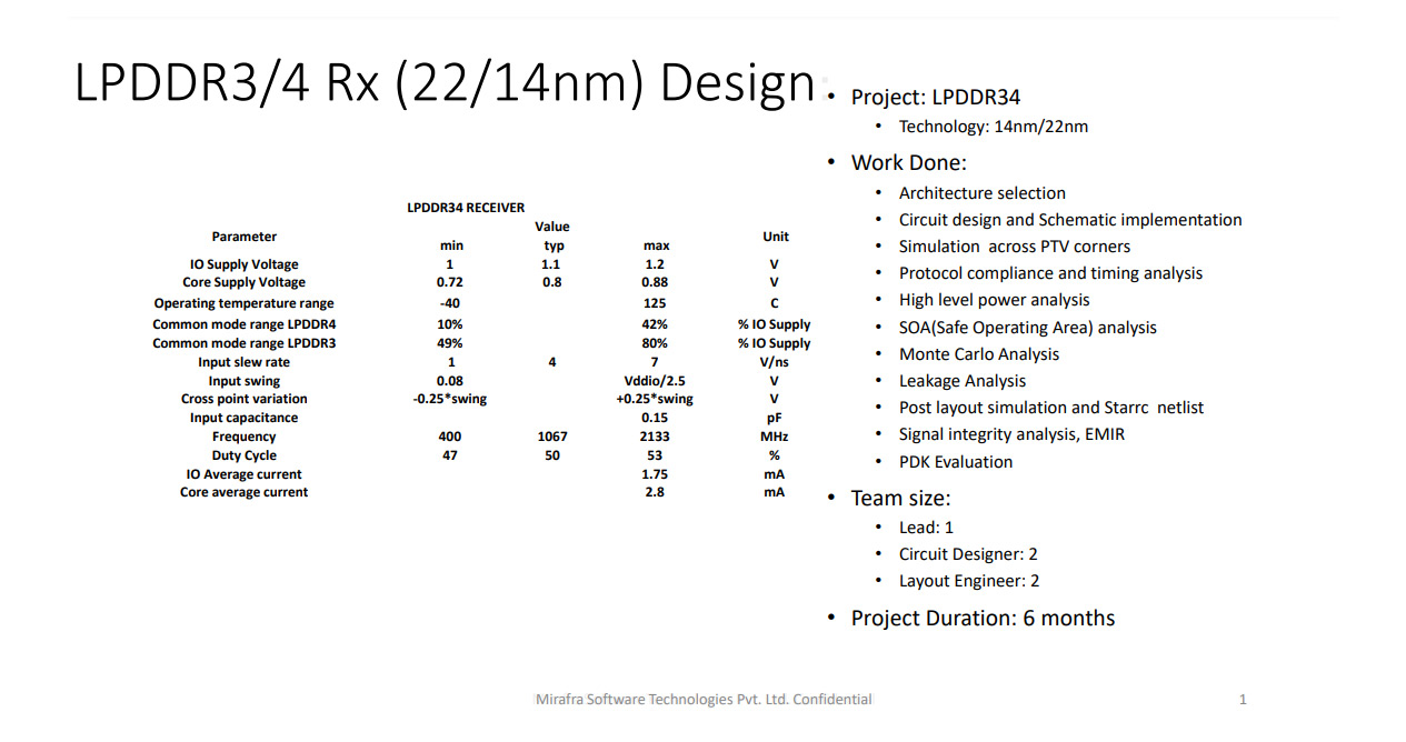
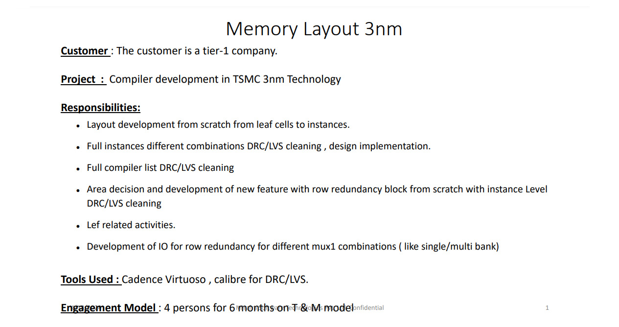
• CPU & Memory Subsystems: Hands-on experience with CPU subsystem integration (ARM/ARC/RISC-V), cache hierarchy, MMU, and memory controller architectures (DDR, LPDDR).
• Low-Power Architecture: Deep understanding of low-power techniques including UPF/CPF, power gating, clock gating, DVFS, multi-voltage designs, and retention strategies.
• RTL Design & Coding Practices: Strong SystemVerilog RTL coding skills with emphasis on reuse, configurability, and synthesis-friendly design.
• Verification & Quality Sign-off: Ability to review and guide verification strategy, static checks test plans, functional coverage, assertions, and regression quality metrics.
• Synthesis, STA & Sign-off: Expertise in synthesis (Design Compiler), static timing analysis, timing closure across multiple PVT corners, and ECO handling.
• Formal & Equivalence Checking: Strong experience with formal verification and logical equivalence checking (LEC).
• DFT & Debug: Good working knowledge of DFT architectures (scan, MBIST, JTAG) and debug/trace infrastructures.
• Post-Silicon Bring-up: Experience with silicon bring-up, lab debugging, silicon validation, and correlation between RTL, simulation, and silicon behavior.
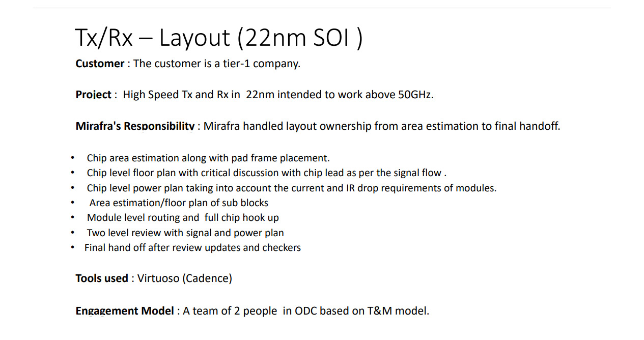
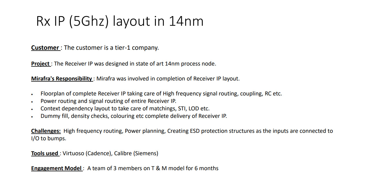
• Chip IO & Packaging: Understanding of chip IO planning, pad ring integration, signal integrity considerations, and packaging constraints.
• Cross-Functional Leadership: Ability to work closely with PD, DV, DFT, firmware, and software teams to ensure seamless execution and delivery.
• Mentoring & Technical Leadership: Proven capability to mentor engineers, review designs, drive best practices, and own delivery of complex SoC programs.
Job Requirement:
• SoC & Micro-Architecture: End-to-end Consumer SoC architecture and micro-architecture design optimized for PPA and real-world use cases.
• CPU & Interconnects: Integration of ARM/ARC/RISC-V CPU subsystems, cache hierarchies, AXI/AHB/APB, and coherent interconnects.
• Memory & High-Speed Interfaces: DDR/LPDDR subsystems and consumer interfaces such as PCIe, USB, Ethernet, CXL, MIPI, and display.
• Low-Power Design: Expertise in UPF-based low-power architecture, clock/power gating, DVFS, and multi-voltage domains.
• RTL, Verification & Sign-off: Strong SystemVerilog RTL, synthesis, STA/timing closure, formal (LEC), and DV/coverage review.
• Post-Silicon & Leadership: Silicon bring-up/debug experience with strong technical leadership and cross-functional collaboration.
Experience (years) : 10+ years
Education Qualification:
BTECH/MTECH in Electrical/Electronics/Computer Science Engineering or Equivalent