- Home
- About us
- Services
- Semiconductors
- Analog and mixed signal
- Bench characterization
- Design verification
- Design for testability (DFT)
- FPGA design
- IC Packaging
- In-house silicon validation lab
- Prototyping and Emulation
- Physical Design
- RTL Design
- Signoff flows
- Silicon Validation
- Synthesis and STA
- Test and Product Engineering
- Product Solutions
- Embedded
- Software
- Semiconductors
- Industries
- Our team
- Career
- Community
- Resources
- Contact us
Mirafra Software Technologies Pvt Ltd is ISO 9001:2015 (Quality Management System) and ISO 27001:2022 (Information Security Management System) certified Company.
TSMC 22nm ULP
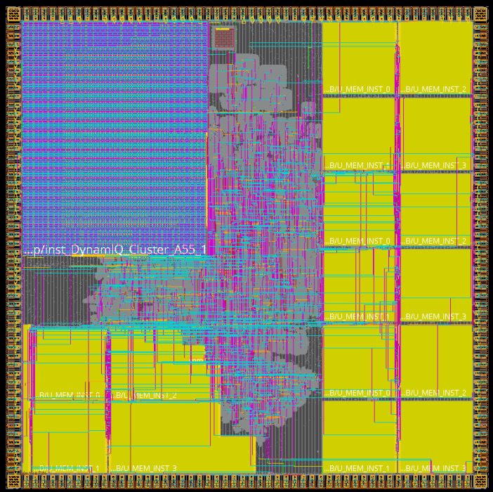
Ramanujan SoC
Mirafra’s IoT SoC Platform developed from scratch, architecture to silicon and everything in between. Complete Hardware and Software stack. Taped out in December, 2025.
Custom Architecture,
Custom IPs & VIPs
Custom IPs & VIPs
In-house RTL to GDS Flow
Silicon Validation @
In-house ESD-safe lab
In-house ESD-safe lab
In-house Custom Software Drivers
0
Million
Gates
0
Million
Instances
0
Macros
0
mm2
Die Size
Silicon Specification Highlights
A complete real-world, application-grade architecture for IoT. Integrating dual processors, full peripheral set, and custom in-house IPs.
Application Processor
Arm Cortex-A55 @ 1.1 GHz
Linux kernel 6.13
Linux kernel 6.13
System Processor
InCore Azurite RISC-V @ 100 MHz
Zephyr 4.1
Always ON System Control Processor
Zephyr 4.1
Always ON System Control Processor
Peripherals
UART · SPI · I2S · GPIO · PWM · Display
Camera · I2C · SDRAM
Camera · I2C · SDRAM
Custom In-House IP
IPC · SCR · HW State machine
Clock & Reset controler · I/O Mux
Display & Camera Contoller
Time Stamp Generator · I2C
Clock & Reset controler · I/O Mux
Display & Camera Contoller
Time Stamp Generator · I2C
Interconnect
Two Independent ARM NI-700 NoC
AXI-Based Communication
AXI-Based Communication
Memory Subsystem
4MB on-chip SRAM Application sub-system
128KB on-chip SRAM System Processor
64MB SDRAM
128KB on-chip SRAM System Processor
64MB SDRAM
Debug Infrastructure
CoreSight Debug
JTAG · SWD
JTAG · SWD
Software Stack
Linux Kernal 6.13 & Zephyr 4.1
BSP · Device Drivers
OS Porting & Customization
BSP · Device Drivers
OS Porting & Customization
Multimedia Stack
Camera - Display
Audio Encoding/Decoding
Video Encoding
End-to-End streaming stack
Audio Encoding/Decoding
Video Encoding
End-to-End streaming stack
Connectivity Stack
IOT edge connectivity
Wi-Fi support
Wi-Fi support
Foundry
TSMC 22nm ULP
13.95 mm2 die size
Ultra-low power process
13.95 mm2 die size
Ultra-low power process
Where We Are Today
Successful GDSII submission, fabrication at TSMC, and silicon shipment are now complete. We are currently awaiting packaged silicon for validation and software bring-up.
Project Kick-off
21st Feb '25
Shipment from TSMC
1st Apr '26
Qual
~ 1st Aug '26
1
2
3
4
5
Tape-out
30th Dec '25
Packaging
8th Jun '26
Complete
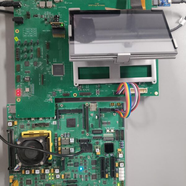
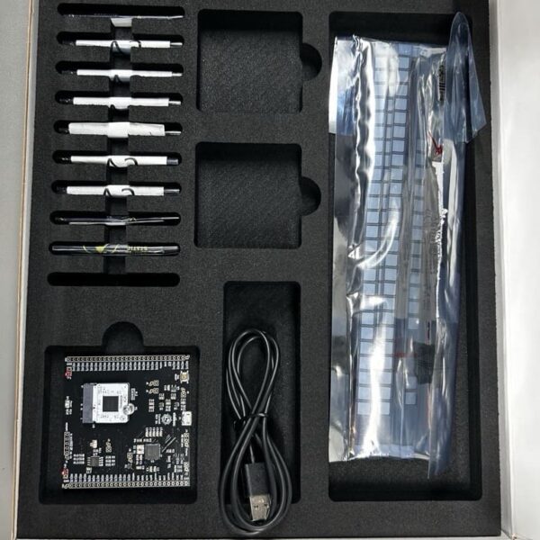
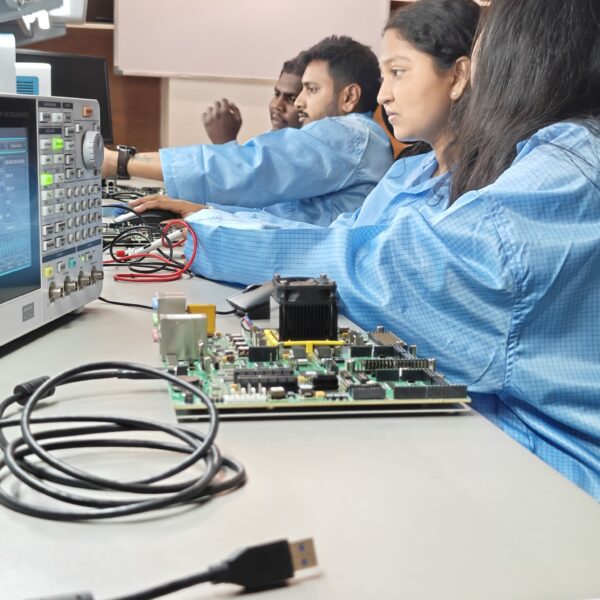
FPGA Prototyping
RTL Design successfully emulated on customized FPGA board with early Zephyr RTOS & Linux OS bring-up.
Complete
Tapeout
Completed tapeout with GDSII/OASIS files and PDK compliance checks.
Complete
Fabrication & Shipment
Silicon fabrication completed at TSMC on the 22nm ULP process node. Full wafer lot shipped to packaging partner.
In Progress
Packaging & Boards
IC Packaging and test board assembly undergoing with manufacturing partners.
Yet To Start
Post-Silicon Validation
Chip bring-up and functional validation at Mirafra's in-house ESD-safe silicon validation lab.
Yet To Start
Software Bring-up on Silicon
Zephyr RTOS and Linux OS bring-up on the evaluation board.
End-to-End Silicon Lifecycle Ownership
Driving end-to-end silicon execution from initial architecture and design through to tape-out, validation, and software bring-up
Phase 1
Specification
Architecture & Micro-Architecture
Phase 2
Logic Design
RTL Design & Verification, DFT
Phase 3
Physical Implementation
Synthesis & PnR
Phase 4
Sign-Off
STA & Physical Verification
Phase 2
Prototype Board Design
Board Design parallel to RTL
Phase 3
Emulation
FPGA Prototyping on an ARM MPS4 board
Phase 4
Validation,
SW Bring-up
SW Bring-up
PSV & Software Development, System stress test
Sign-off Review
Review of Coverage, Regression, GLS, Bug Closures, Stress and Stability Test Results
Phase 5
Tape Out
GDSII, OASIS Submission to TSMC
Phase 6
Packaging
IC Packaging
What Makes Ramanujan SoC Special
The Ramanujan SoC is Mirafra's internal showcase of full-stack silicon development capability - delivered at production quality, under an aggressive timeline, with fully in-house program management.
Targeting IoT edge applications such as smart doorbells, the chip integrates a hetrogenous dual core architecture - combining rich media processing with secure, deterministic system management in a single, power-optimized silicon solution.
This milestone demonstrates something remarkable: a global design services company that can define, own, and deliver turnkey end-to-end silicon - from architecture through physical design, software bring-up, and validation. We didn't just execute a piece of a project; we owned the entire journey.
⏱️
10 months start-finish
Concept to tape-out in an accelerated timeline
Iterative, Milestone-Driven Development
🔁
Incremental RTL & Testbench Releases
Progressive releases from v0.1 → v1.0 with continuous DV, FPGA, and PD feedback through structured JIRA flow and detailed review mechanism.
🧩
Early FPGA-Based Pre-Silicon Validation
Complete SoC emulation on FPGA with custom hardware extensions enabled software bring-up before silicon availability.
📊
Progressive Closure Across All Domains
Coverage, timing, and power targets closed progressively — culminating in zero critical bugs in final pre-tape-out weeks.
✅
Parallel Cross-Functional Coordination
Individual teams worked in parallel with structured milestone reviews and seamless handoffs, ensuring no bottlenecks.
Engineering Solutions Behind Ramanujan SoC
Designing the Ramanujan SoC from scratch under stringent cost and timeline targets required complete end-to-end silicon ownership while overcoming complex technical and execution challenges.
Built Multi-Vendor EDA Flow & Methodology
Integrated tools from multiple EDA vendors to optimize quality across domains. Established consistent signoff criteria, convergence metrics, and created internal documentation, methodologies, and handoff templates from scratch.
Dual-Processor Architecture with Pin-Optimized IP Strategy
Selected ARM Cortex-A55 + RISC-V Azurite dual-processor. Used ARM NI-700 NoC for isolated domain management. Offloaded Wi-Fi/BT/Zigbee to external modules via SPI/UART to minimize die area and complexity.
Cross-Functional Convergence in Lockstep
Architecture, design, verification, software, and physical implementation teams worked in lockstep across 2 parallel tracks. Structured ECO cycles and milestone reviews ensured no handoff gaps across all 10+ verticals.
Full Specification Ownership & Decision Authority
Mirafra owned the end-to-end architecture definition, interface specifications, integration boundaries, and testability features — proactively making decisions, resolving ambiguities, and defending trade-offs using collective domain expertise.
DFT, BIST & Full Validation Infrastructure
Implemented full scan insertion, ATPG, MBIST, CoreSight debug hooks, FPGA emulation, and silicon diagnostics upfront. 100% coverage closure on custom IPs.
Proactive De-risking & Parallel Execution
Upfront schedule planning, technical risk buffers, and active de-risking via early FPGA prototyping. Parallel RTL, DV, FPGA, and PD execution with structured ECO cycles — achieving tapeout in 10 months with zero critical bugs.
Cost & Timeline Optimized
SoC Execution
SoC Execution
Enabled faster and cost-efficient industry-grade silicon development through strategic IP selection, simplified custom logic, external subsystem offloading, multi-vendor EDA flow optimization, concurrent cross-functional execution, and upfront DFT/emulation infrastructure — minimizing silicon complexity, reducing rework cycles, and accelerating first-time-right tapeout readiness.
"
"The Ramanujan SoC demonstrates true end-to-end semiconductor capabilities. It showcases our ability to take complex designs from concept to silicon and deliver them along with the complete software stack."
PV Shyam Sunder Rao
MD & Co-Founder, Mirafra Technologies
"The successful tapeout of the Ramanujan SoC by the Mirafra team is a significant milestone for the Indian semiconductor design services ecosystem, which is evolving from being merely backend outsourcing vendors to fully owning end-to-end turnkey chip design! We are pleased that our Azurite RISC-V core serves as the system management backbone for this design. This engagement highlights the growing maturity of indigenous semiconductor IP and the strength of collaborations that bring together design services and product-grade innovation in India."
GS Madhusudan
Co-founder & CEO, InCore Semiconductors
Mirafra Built for Silicon Excellence
The One-Stop Partner for Turnkey ASIC Development
Capability Expansion &
Scalability
We have established comprehensive end-to-end SoC architecture and program management capabilities. Our strategic vendor collaborations and in-house ASIC flow deliver cost effective solutions with optimized power, performance and area. Our seamless hardware-software alignment enables us to meet diverse end application needs
Strategic Differentiation
We go beyond service provision to complete turnkey solutions Mirafra has evolved into a full spectrum semiconductor partner capable of spec-to-silicon-to-system execution. This reflects our ambition to be the leader in the niche landscape of end to-end turnkey semiconductor solutions.
Organizational Commitment
We have invested in building a multidisciplinary team with specialized end-to-end execution expertise, and strong ecosystem partnerships with Board Manufacturing & Assembly, Packaging, Fabrication, IP and Tools vendors.
Ramanujan SoC in News
Explore the latest news, updates, and media mentions of Ramanujan SoC.
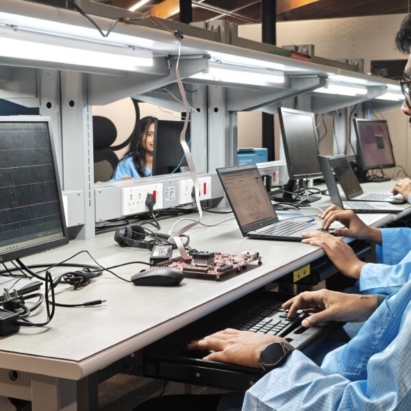
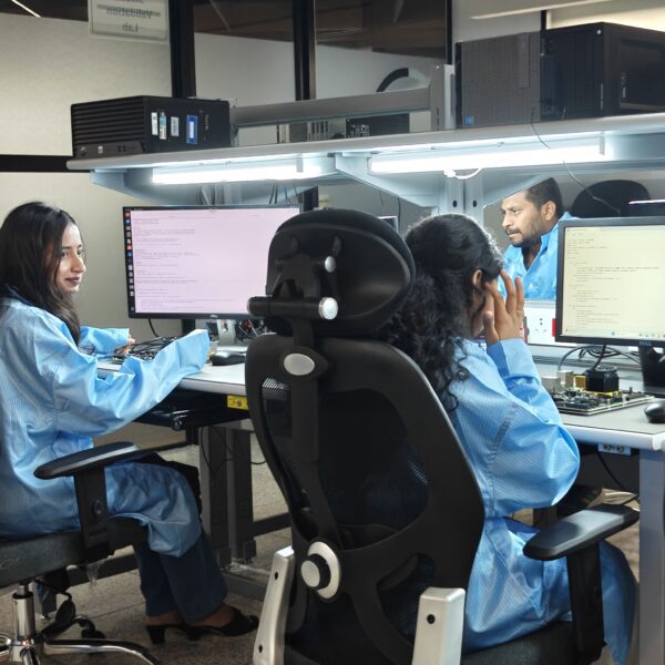
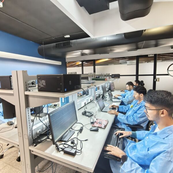
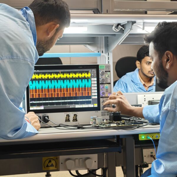
Defined by Design, Proven by Silicon
Showcasing the robust prototyping environment and final-form hardware of the Ramanujan platform.
Turnkey ASIC Partner
Partner with Mirafra
for Your Next SoC
From architecture definition to silicon validation and software bring-up, Mirafra delivers production-ready SoC solutions with proven in-house expertise, complemented by strong semiconductor ecosystem partnerships across the complete silicon lifecycle.
Start Your ASIC Journey
Talk to our silicon experts and explore how Mirafra can accelerate your next chip program.
Connect with Our Team Explore all services →